Theory of X-Ray Photoelectron Spectroscopy
Introduction
X-Ray Photoelectron Spectroscopy (XPS), also known as Electron Spectroscopy for Chemical Analysis (ESCA), is the most widely used surface analysis technique because of its relative simplicity in use and data interpretation. XPS is used to obtain chemical information about the surfaces of solid materials. Both composition and the chemical state of surface constituents can be determined by XPS. Insulators and conductors can easily be analyzed in surface areas from a few microns to a few millimeters across. XPS spectra are obtained by irradiating a material with a beam of X-rays while simultaneously measuring the kinetic energy and number of electrons that escape from the top 1 to 10 nm of the material being analyzed. XPS requires ultra high vacuum (UHV) conditions.
Basic Principle
XPS was developed in the mid 1960s by K. Siegbahn and his research group. K. Siegbahn was awarded the Nobel Prize for Physics in 1981 for his work in XPS. The phenomenon is based on the photoelectric effect outlined by Einstein in 1905 where the concept of the photon was used to describe the ejection of electrons from a surface when photons impinge upon it. For XPS, Al Kalpha (1486.6eV) or Mg Kalpha (1253.6eV) are often the photon energies of choice.
Photoelectron spectroscopy is based upon a single photon in/electron out process and from many viewpoints this underlying process is a much simpler phenomenon than the Auger process. The energy of a photon of all types of electromagnetic radiation is given by the Einstein relation: E=hv
Photoelectron spectroscopy uses monochromatic sources of radiation (i.e. photons of fixed energy). In XPS the photon is absorbed by an atom in a molecule or solid, leading to ionization and the emission of a core (inner shell) electron. The kinetic energy, EK of the emitted photoelectrons can be determined by the energy of the X-ray radiation and the electron binding energy, EB, as given by: EK=hv-EB
The experimentally measured energies of the photoelectrons are given by: EK= hv-EB -Φ , whereΦ is the work function of the spectrometer. Below Fig. 1a & 1b show the principle of photoelectron generation.

Fig. 1a The principle of photoelectron generation
 Fig.1b – The diagram showing the process of photo-emission
XPS instruments consist of an X-ray source, an energy analyzer for the photoelectrons, and an electron detector. Fig. 2a & 2b illustrate the configuration of the focused X-ray source and energy analyzer. The electron gun scans the X-ray anode (Al Anode) with a finely focused electron beam, stimulating the emission of X-rays from the anode. Rastering the electron beam over an area of the anode produces a complementary rastering X-ray beam. A Quartz crystal monochromator that focuses and scans the image results from the rastering X-ray beam upon the sample surface. For sample neutralization, the electron beam scans the anode surface at very high speed to reduce differential charging effects that cause data interpretation problems with non-conductive samples.

Fig. 2a – Configuration of the Focused X-Ray Source and the Energy Analyzer

Fig. 2b – The technique of focusing and scanning X-ray
Application of XPS
Example 1 - Fig. 3 shows XPS raw peak intensity map for fluorine, showing the 150 analysis points and a region on the hard disk where the lubricant is missing.

Fig. 3 – XPS raw peak intensity map for fluorine
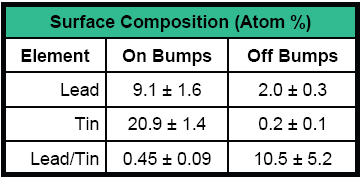
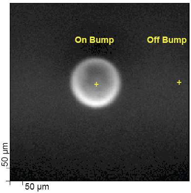
Example 2 - Fig. 4 shows the characterization of the surface composition of both the solder bumps and the interbump region by 7.5μm diameter scanned x-ray probe beam XPS. XPS spectra collected on and off solder bumps showed that the die surface was contaminated by high levels of lead, presumably from the solder paste reflow process.
|
(a) |
 |
(b) |
 |
| Fig. 4 – Characterizing Bumped Wafers with XPS |
|||
| (a) Quantitative summary of the analysis | (b) Scanned x-ray beam induced secondary electron image of a solder bump | ||
Example 3 - Fig. 5 shows High resolution C 1s and O 1s spectra of PET after a 500V Ar ion beam sputter and 10kV C60 ion beam. From Fig. 5(a), as sputtering continues the O 1s spectra show a loss of total O as a function of depth. In a similar manner, the C 1s spectra show a loss of O containing C species. Together the O and C spectra show the chemical damage that occurs when sputtering. From Fig. 5(b), C 1s and O 1s spectral shapes remain nearly constant as a function of sputter depth while etching with the C60 ion beam. C60 sputter ion gun becomes very important to provide the ability to remove surface contaminants from polymer surfaces and to depth profile organic thin films while causing minimal damage to the remaining surface.
| (a) |  |
(b) |  |
| Fig. 5 - High resolution C 1s and O 1s spectra of PET after (a) 500V Ar ion beam and (b) 10kV C60 ion beam | |||
Summing-up
XPS is a surface analysis technique with a sampling volume that extends from the surface. Alternatively, XPS can be utilized for sputter depth profiling to characterize thin films by quantifying matrix-level elements as a function of depth. XPS is an elemental analysis technique that is unique in providing chemical state information of the detected elements, such as distinguishing between sulfate and sulfide forms of the element sulfur. XPS routinely used to analyze inorganic compounds, metal alloys, semiconductors, polymers, elements, catalysts, glasses, ceramics, paints, papers, inks, woods, plant parts, make-up, teeth, bones, medical implants, bio-materials, viscous oils, glues, ion modified materials and many others.
For more details, please visit our Brochure or Application Notes.

