
Germany Fraunhofer IPMS institute introduced PHI hard X-ray photoelectron spectroscopy
Insight into Nano Depth - New Fraunhofer IPMS X-ray photoelectron spectrometer enables tiny particle analysis
We are in an era of rapid development of information technology, which chips can be described as an artificial intelligence nerve cell, transmitting important information and signals to smart devices through billions of tiny components inside. Nowadays, the semiconductor chips built in smart devices are getting smaller. However, their functions are getting more powerful and higher efficiency.
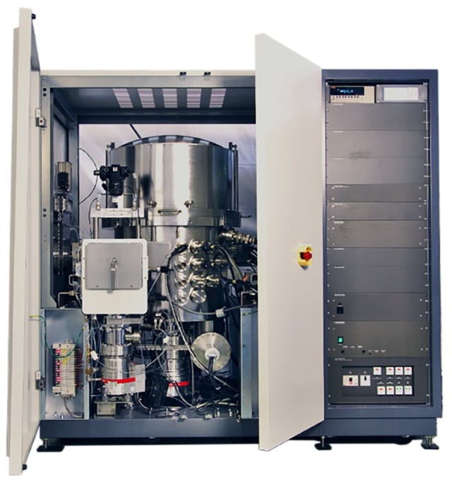
Since the nano-scale surface structure can no longer be recognized by the naked eye, in order to analyze the surface characteristics of silicon wafers in the nanometer depth range, Fraunhofer Institute for Photonic Microsystems (Fraunhofer IPMS) purchased a high-performance hard X-ray photoelectron spectrometer (XPS) from PHI Electronics GmbH.
Dr. Benjamin Uhlig, principal investigator of the Fraunhofer IPMS Institute said “PHI's new Quantes hard X-ray photoelectron spectrometer can detect surface features, film structures and surface contaminants in the nanometer depth range without causing any damage. In order to accurately analyze the chemical composition on the surface of the chip, it is very important to detect the nano-depth area. This new feature of XPS will allow everyone to clearly understand the manufacturing process of semiconductor chips. It will play a key role in optimizing chip performance in the future.”
The Hard X-ray photoelectron spectroscopy (XPS) by Physical Electronics GmbH
Another advantage of this new XPS instrument is versatility. In addition to using the Al-ka X-ray source (1486 eV) for conventional XPS measurements, we can conduct analytical experiments that extend deeper. The system is equipped with a Cr-ka X-ray source (5414 eV), which can provide an analysis depth of about 22 nanometers to the Si chip. It is three times the conventional XPS detection depth (about 7 nanometers) based on Al-ka X-rays.Dr. Benjamin Uhlig said “Through the hard X-ray photoelectron spectroscopy, we can analyze transition metals well. The system can clean the sample surface and also perform depth profile analysis. In addition, it can also perform XPS test analysis of samples from -120°C to 300°C with variable temperature and experiments with potential contact samples. "
The secondary electron imaging (SXI) of the system can locate very small structures on the sample accurately. The hard X-ray XPS system of the Fraunhofer IPMS Institute can be used for extensive comprehensive analysis. At the same time, the Fraunhofer IPMS has provided various cooperation opportunities in product development for major companies in the world.The Fraunhofer IPMS invested in a hard x-ray photoelectron spectrometer as part of German microelectronics research project. This investment is funded by the Federal Ministry of Education and Research and aims to promote Germany into a science and technology center.
Background information
The Fraunhofer Institute for Photonic Microsystems (Fraunhofer IPMS) locates in Dresden, Germany, provides future-oriented solutions for industrial manufacturing and automation, as well as medical technologies that improve the quality of life. Fraunhofer IPMS has more than 350 scientists and engineers who have demonstrated the highest level in the fields of optical sensors and actuators, integrated circuits, wireless data communications and microelectronics.
Information Sources:
https://www.ipms.fraunhofer.de/en/press-media/press/2020/X-ray-photoelectron-spectrometer.html